ATmega Pt.2: ADC and controlling an LCD
After we've built  a minimal microcontroller system based on the ATmega 1284p chip, we're now going to
Here's what my breadboard looks like:
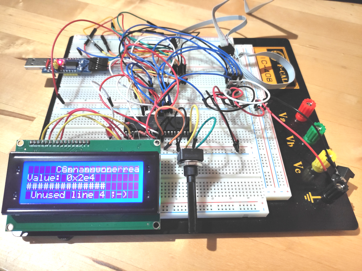
At the bottom of the board is the 20x4 character LCD module and right next to it the 10k potentiometer for the ADC.
The LCD is driven by the very popular Hitachi HD44780U controller chip in combination with a I2C LCD adapter based on the 8bit TCA9534 I2C I/O expander chip.
Here's the complete schematic:
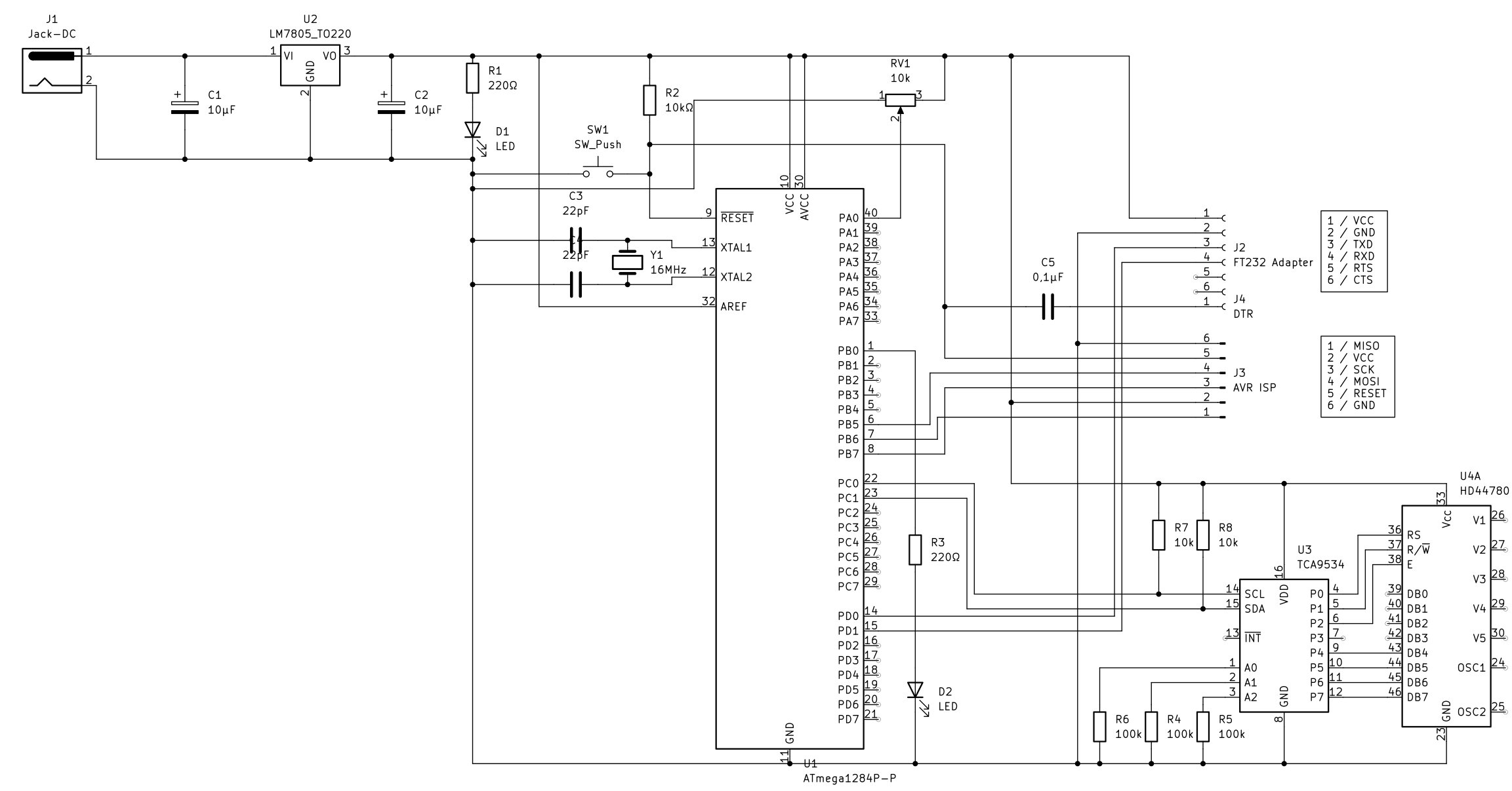
It's not strictly complete because it only contains the TCA9534 I/O expander and HD44780U controller chips; the actual LCD is missing, but for our intents and purposes, only the LCD controller is relevant.
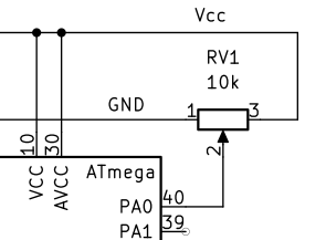
The sliding contact of the 10k potentiometer is connected to pin 40 (ADC0, which is the first of 8 ADCs) of the ATmega chip. The other two pins are connected to Vcc/AREF (reference voltage) and GND, thereby forming an adjustable voltage divider:
The LCD is controlled by a HD44780U LCD controller chip using an 8bit bus interface with 3 control pins:
These pins are exposed on the LCD module like this:
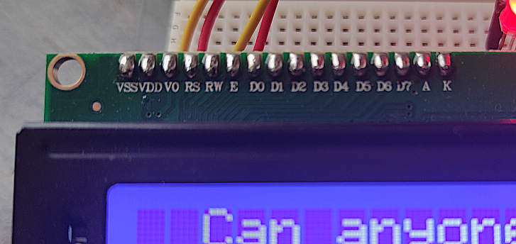
The other pins of the LCD module are:
These pins are taken care of by the I2C expander module.
So, for programming the LCD controller, we need 11 I/O pins in total: D0..D7, E, R/W and RS. Luckily, the controller can be operated in 4bit instead of the 8bit mode, transferring an 8bit word in two read/write cycles with 4 bits each. Only the upper 4 bits (DB4..DB7) are used. This reduces the total number of necessary I/O pins to only 7 (4 data pins, 3 control pins).
Since the ATmega MPU is equipped with an I2C serial bus interface, we can use an 8bit I/O expander chip like the TCA9534. Such an expander accepts 8bit data words through its serial I2C interface and puts them on its I/O pins P0..P7 in parallel. That is sufficient to control the LCD controller.
Here's the part of the schematic which shows the interfacing with the LCD controller:
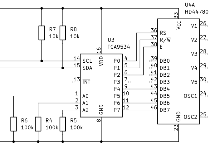
There are two pullup resistors R7 and R8 on the SCL and SDA lines because the bus master on an I2C bus transmit signals by connecting the lines with GND.
The I2C device ID of the TCA9534 I/O expander is configured via its pins A0..A2. These represent the lower 3 bits of the whole 7-bit device ID. The upper 3 bits are hard-wired internally to 0100. So the whole 7-bit device ID is:
In our schematic above you can see that A0..A2 are all pulled down to GND which means that the device ID is 0b0100000 or 0x20.
The TCA9534 expander has 4 internal 8bit registers. Communicating with it via I2C involves writing 8-bit values to any of its 4 registers by first sending the register number and then the data value.
Consequently, here's the process of writing an 8bit value V to a TCA9534 register R:
For interfacing with the HD44780U LCD controller, we'll only ever need to write data bytes to the TCA9534 expander's output pins. Therefore we need to initialize register 3 (configuration of data direction) with 0x00 (all output) and then write to register 1 to output data.
The internal ADCs are described in detail in chapter 23 of the ATmega 1284p's datasheet. It is possible to use the ADCs in interrupt mode or polling mode. For simplicity's sake, we're going to use the polling mode.
Polling one of the 8 ADCs involves using 3 memory-mapped registers: ADMUX, ADCSRA and ADC. These registers are described in chapter 23.9 of the datasheet.
Bits MUX0..MUX4 (bits 0..4) of the ADMUX register select the number of the ADC and the GAIN value. There are 8 ADCs available in the 1284p, so we set MUX0..2 to a number between 0 and 7 and set MUX4 and MUX5 to 0.
The ACLAR bit of the ADMUX register selects the adjustment of the 10-bit ADC result in the 16-bit ADC data register. 0 means right-adjust and 1 means left-adjust. We typically set this to 0.
The REFS0..REFS1 bits select the reference voltage according to the following table:
As you can see in the schematic above, we're using an external voltage reference at the AREF pin, so we just set both REFS0 and REFS1 to 0.
The ADPS (ADC Prescaler Select Bits) are defined as:
In order to convert and poll a single value from an ADC, we have to do the following:
This function returns a 16bit value ranging from 0 to 1023, reflecting the voltage at the ADC pin ranging from 0v to AREF.
First of all we need to get to know how to program the I2C (or TWI) interface on the ATmel MPU. There are four relevant registers: TWBR, TWCR, TWSR and TWDR. They're all described in chapter 21.9 of the ATmega 1284p datasheet. There's also a good introduction into I2C programming on the ATmega here
I divided I2C communication into 4 parts: initialization, generate START condition, write byte and generate STOP condition.
I2C Initialization:
We configure the I2C prescaler and the bitrate.
Also, we enable I2C by setting the TWEN bit to 1 in the TWCR register.
Generate I2C Start Condition:
The TWINT bit of the TWCR register indicates whether the I2C interface has finished its current operation. We clear it by writing 1 to it. Also, we set the TWSTA bit to 1 in order to generate a START condition and set the TWEN bit to 1 to enable the I2C interface.
After that, we wait until the operation has finished by waiting until the TWINT bit of the TWCR register is 1.
I2C Write Byte:
We write the data byte to the TWDR (TWI Data) register.
In the TWCR register, we set the TWEN (TWI Enable) bit to 1 for enabling I2C and start the send operation by clearing the TWINT (TWI Interrupt) bit.
The hardware then shifts the data byte over the SDA/SCL pins. When that operation has finished, the TWINT bit of the TWCR register will be set to 1. This is what we wait for in the while loop.
Generate I2C Stop Condition:
This is similar to generating the start condition, except that we use the TWSTO bit rather than the TWSTA bit, and we don't wait for the operation to finish.
Now that we have basic communication functions via I2C, we can write a function to initialize the TCA9534 and HD44780U:
Note that we gently wait for a short period each time after writing something into a TCA9534 register.
Directly after startup, the HD44780U controller is in 8bit mode, so we need to switch it to the 4bit mode:
Now in order to understand this, we need to consider two things:
So in order to write the upper 4 bits of data (for example: 0011) to the HD44780U controller, we need to set the 8 data output lines of the TCA9534 to the following values, ordered by time:
We set the upper 4 data bits, R/W to 0 (=write), RS to 0 (=instruction) and then let E toggle from 0 to 1 to 0. This signals the HD44780U to accept the instruction byte. Bit 3 (the one marked with '--' above is used by the I2C expander board to control the background light.
This is what it looks like in code:
The next thing we do is to write the function lcd_set() to write 8bit data words to the HD44780U which can conveniently distinguish between 4bit and 8bit mode:
The rs parameter represents the R/S line. 0 means instruction and 1 means data.
The d parameter represents the entire 8bit data word to write to the HD44780U controller.
That means if the controller is in 4bit mode (upperNibbleOnly=0), the data word will be written in two parts: upper 4bits first, then the lower 4bits. If the controller is in 8bit mode (upperNibbleOnly=1), the data word will be written in a single cycle. Of course, since only the upper 4 data lines of the controller are connected to the TCA9534, the controller won't see the lower 4 bits.
With all this in place, we can start writing instructions and character data to the HD44780U. Again, it is strongly advised to refer to the instruction table in the HD44780U datasheet.
A simple example is the "Clear Display" instruction 0x01:
Or a slightly less simple example the "Set DDRAM Address" instruction 0x80 (the lower 7 bits represent the actual address):
Another one would be the to write a data byte to the DDRAM:
The DDRAM is where you write your character data in ASCII encoding.
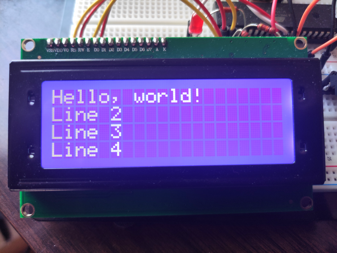
Here's a small "Hello, world!" example which conveniently uses the C functions I have implemented:
Here's what it looks like in real-life:
And the final Demo which reads the ADC and prints the converted value on the LCD:
The complete source code of the ADC/LCD Demo:
avr_adc_lcd_demo.tar.gz (14kb)
A very good and thorough introduction into I2C communication by Texas Instruments:
sbaa565.pdf
The Hitachi HD44780U LCD controller datasheet:
HD44780.pdf
The Microchip ATmega 1284 datasheet:
ATmega164A_PA-324A_PA-644A_PA-1284_P_Data-Sheet-40002070B.pdf
The Texas Instruments TCA9534 8bit I/O expander datasheet:
tca9534.pdf
a minimal microcontroller system based on the ATmega 1284p chip, we're now going to- use one of the controller's internal analog-to-digital converters (ADC) to input some value using a potentiometer
- interface with an LCD via I2C to output the digitized value in textual form
Here's what my breadboard looks like:

At the bottom of the board is the 20x4 character LCD module
and right next to it the 10k potentiometer for the ADC.The LCD is driven by the very popular Hitachi HD44780U
controller chip in combination with a I2C LCD adapter based on the 8bit TCA9534 I2C I/O expander chip.Here's the complete schematic:
It's not strictly complete because it only contains the TCA9534 I/O expander and HD44780U controller chips; the actual LCD is missing, but for our intents and purposes, only the LCD controller is relevant.
The sliding contact of the 10k potentiometer is connected to pin 40 (ADC0, which is the first of 8 ADCs) of the ATmega chip. The other two pins are connected to Vcc/AREF (reference voltage) and GND, thereby forming an adjustable voltage divider:
Interfacing with the 20x4 Character LCD
The LCD is controlled by a HD44780U LCD controller chip using an 8bit bus interface with 3 control pins:
| Pin | Description |
|---|---|
| RS | Register select (0=command, 1=data) |
| R/W | Read/!Write (0=Write, 1=Read) |
| E | Clock enable (falling-edge triggered) |
| DB0..DB7 | Data Bit 0..7 |
These pins are exposed on the LCD module like this:
The other pins of the LCD module are:
- A (Anode), K (Cathode) of the background light
- VSS, VDD: supply voltage and ground
- V0: contrast adjustment of the display
These pins are taken care of by the I2C expander module.
So, for programming the LCD controller, we need 11 I/O pins in total: D0..D7, E, R/W and RS. Luckily, the controller can be operated in 4bit instead of the 8bit mode, transferring an 8bit word in two read/write cycles with 4 bits each. Only the upper 4 bits (DB4..DB7) are used. This reduces the total number of necessary I/O pins to only 7 (4 data pins, 3 control pins).
Since the ATmega MPU is equipped with an I2C serial bus interface, we can use an 8bit I/O expander chip like the TCA9534. Such an expander accepts 8bit data words through its serial I2C interface and puts them on its I/O pins P0..P7 in parallel. That is sufficient to control the LCD controller.
Here's the part of the schematic which shows the interfacing with the LCD controller:
There are two pullup resistors R7 and R8 on the SCL and SDA lines because the bus master on an I2C bus transmit signals by connecting the lines with GND.
The I2C device ID of the TCA9534 I/O expander is configured via its pins A0..A2. These represent the lower 3 bits of the whole 7-bit device ID. The upper 3 bits are hard-wired internally to 0100. So the whole 7-bit device ID is:
| 0 | 1 | 0 | 0 | A2 | A1 | A0 |
In our schematic above you can see that A0..A2 are all pulled down to GND which means that the device ID is 0b0100000 or 0x20.
The TCA9534 expander has 4 internal 8bit registers. Communicating with it via I2C involves writing 8-bit values to any of its 4 registers by first sending the register number and then the data value.
Consequently, here's the process of writing an 8bit value V to a TCA9534 register R:
- Generate START condition: pull SDA low, then pull SCL low
- Send the device ID and R/W bit (the actual ID is in bits 7..1; bit 0 indicates a read (1) or a write (0)
(i.e. when writing to device 0x20, we send 0x40) - Send the register number R
- Send the data byte V
- Generate STOP condition: pull SCL up, then pull SDA up
| Register | Description |
|---|---|
| 0 | Input Port Reflects the incoming logic levels of the pins |
| 1 | Output Port Shows the outgoing logic levels of the pins |
| 2 | Polarity Inversion Allows polarity inversion of pins defined as inputs by the configuration register (default: 0x00) |
| 3 | Configuration Register Configures the direction of the I/O pins. If a bit in the register is set to 1, the corresponding port pin is configured as an input. If set t0 0, the corresponding pin is configured as output. (default: 0xff) |
For interfacing with the HD44780U LCD controller, we'll only ever need to write data bytes to the TCA9534 expander's output pins. Therefore we need to initialize register 3 (configuration of data direction) with 0x00 (all output) and then write to register 1 to output data.
Programming
Polling the ADC
The internal ADCs are described in detail in chapter 23 of the ATmega 1284p's datasheet
. It is possible to use the ADCs in interrupt mode or polling mode. For simplicity's sake, we're going to use the polling mode.Polling one of the 8 ADCs involves using 3 memory-mapped registers: ADMUX, ADCSRA and ADC. These registers are described in chapter 23.9 of the datasheet.
The ADMUX Register (ADC Multiplexer Selection Register)
| Bit | 7 | 6 | 5 | 4 | 3 | 2 | 1 | 0 |
| Name | REFS1 | REFS0 | ACLAR | MUX4 | MUX3 | MUX2 | MUX1 | MUX0 |
| Read/Write | R/W | R/W | R/W | R/W | R/W | R/W | R/W | R/W |
| Initial Value | 0 | 0 | 0 | 0 | 0 | 0 | 0 | 0 |
Bits MUX0..MUX4 (bits 0..4) of the ADMUX register select the number of the ADC and the GAIN value. There are 8 ADCs available in the 1284p, so we set MUX0..2 to a number between 0 and 7 and set MUX4 and MUX5 to 0.
The ACLAR bit of the ADMUX register selects the adjustment of the 10-bit ADC result in the 16-bit ADC data register. 0 means right-adjust and 1 means left-adjust. We typically set this to 0.
The REFS0..REFS1 bits select the reference voltage according to the following table:
| REFS1 | REFS0 | Voltage Reference Selection |
|---|---|---|
| 0 | 0 | AREF, Internal Vref turned off |
| 0 | 1 | AVCC with external capacitor at AREF pin |
| 1 | 0 | Internal 1.1v Voltage Reference with external capacitor at AREF pin |
| 1 | 1 | Internal 2.56v Voltage Reference with external capacitor at AREF pin |
As you can see in the schematic above, we're using an external voltage reference at the AREF pin, so we just set both REFS0 and REFS1 to 0.
The ADCSRA Register (ADC Control and Status Register A)
| Bit | 7 | 6 | 5 | 4 | 3 | 2 | 1 | 0 |
| Name | ADEN | ADSC | ADATE | ADIF | ADIE | ADPS2 | ADPS1 | ADPS0 |
| Read/Write | R/W | R/W | R/W | R/W | R/W | R/W | R/W | R/W |
| Initial Value | 0 | 0 | 0 | 0 | 0 | 0 | 0 | 0 |
-
Bit 7: ADEN (ADC Enable)
Setting this bit to 1 enables the ADC. -
Bit 6: ADSC (ADC Start Conversion)
In single conversion mode, write one to this bit to start each conversion. In Free Running Mode, write one to this bit to start the first conversion.
When reading this bit, it will be 1 as long as the conversion is in progress. When the conversion is complete, it will return to 0. Writing zero to this bit has no effect. - Bit 5: ADATE (ADC Auto Trigger Enable)
When 1 is written to this bit, Auto Triggering of the ADC is enabled. In that case, the ADC will start a conversion on a positive edge of the selected trigger signal. The trigger source is selected by setting the ADC Trigger Select bits (ADTS) in ADCSRB. - Bit 4: ADIF (ADC Interrupt Flag)
This bit is set when an ADC conversion completes and the Data Register is updated. - Bit 3: ADIE (ADC Interrupt Enable)
When this bit is set to 1 and the I-bit in SREG is set, the ADC Conversion Complete Interrupt is activated. - Bits 2..0: ADPS2..0 (ADC Prescaler Select Bits
These bits determine the division factor betwen the XTAL frequency and the input clock to the ADCl
The ADPS (ADC Prescaler Select Bits) are defined as:
| ADPS2 | ADPS1 | ADPS0 | Division Factor |
|---|---|---|---|
| 0 | 0 | 0 | 2 |
| 0 | 0 | 1 | 2 |
| 0 | 1 | 0 | 4 |
| 0 | 1 | 1 | 8 |
| 1 | 0 | 0 | 16 |
| 1 | 0 | 1 | 32 |
| 1 | 1 | 0 | 64 |
| 1 | 1 | 1 | 128 |
In order to convert and poll a single value from an ADC, we have to do the following:
-
Set the ADMUX register:
- The desired ADC channel number in bits MUX2..0
- The reference voltage selector bits REFS1..0 to 0 (=AREF)
- The bit adjustment bit ADLAR to 0 (=right-adjusted)
-
Set the ADCSRA register:
- The ADC Enable (ADEN) bit to 1 (=enable)
- The ADC Start Conversion (ADSC) bit to 1 (=start conversion)
- The ADC Prescaler Bits (ADPS2..0) to 111 (=7 for dividion factor 128)
- Wait unil the ADIF bit (ADC Interrupt Flag) of the ADCSRA register is 1 (=conversion is complete)
- Read the converted 10bit value from the 16bit ADC register
- Set the ADIF bit (ADC Interupt Flag) of the ADCSRA register to 1
uint16_t readADC( uint8_t chnl )
{
   chnl &= 0x07;
   ADMUX = chnl;
   ADCSRA = ( 1 << ADEN ) | ( 1 << ADSC ) | 0x07;
   while( !( ADCSRA & ( 1 << ADIF ) ) );
   uint16_t adc = ADC;
   ADCSRA |= 1 << ADIF;

   return( adc );

}
This function returns a 16bit value ranging from 0 to 1023, reflecting the voltage at the ADC pin ranging from 0v to AREF.
Controlling the LCD
First of all we need to get to know how to program the I2C (or TWI) interface on the ATmel MPU. There are four relevant registers: TWBR, TWCR, TWSR and TWDR. They're all described in chapter 21.9 of the ATmega 1284p datasheet
. There's also a good introduction into I2C programming on the ATmega here I divided I2C communication into 4 parts: initialization, generate START condition, write byte and generate STOP condition.
I2C Initialization:
void i2c_init()
{
   TWSR = 0x00;
   TWBR = ( F_CPU / 100000 ) - 8;
   TWCR = ( 1 << TWEN );
}
We configure the I2C prescaler and the bitrate.
Also, we enable I2C by setting the TWEN bit to 1 in the TWCR register.
Generate I2C Start Condition:
void i2c_start()
{
   TWCR = ( 1 << TWINT ) | ( 1 << TWSTA ) | ( 1 << TWEN );
   while( ( TWCR & ( 1 << TWINT ) ) == 0 );
}
The TWINT bit of the TWCR register indicates whether the I2C interface has finished its current operation. We clear it by writing 1 to it. Also, we set the TWSTA bit to 1 in order to generate a START condition and set the TWEN bit to 1 to enable the I2C interface.
After that, we wait until the operation has finished by waiting until the TWINT bit of the TWCR register is 1.
I2C Write Byte:
void i2c_write( uint8_t d )
{
   TWDR = d;
   TWCR = ( 1 << TWINT ) | ( 1 << TWEN );
   while( ( TWCR & ( 1 << TWINT ) ) == 0 );
}
We write the data byte to the TWDR (TWI Data) register.
In the TWCR register, we set the TWEN (TWI Enable) bit to 1 for enabling I2C and start the send operation by clearing the TWINT (TWI Interrupt) bit.
The hardware then shifts the data byte over the SDA/SCL pins. When that operation has finished, the TWINT bit of the TWCR register will be set to 1. This is what we wait for in the while loop.
Generate I2C Stop Condition:
void i2c_stop()
{
   TWCR = ( 1 << TWINT ) | ( 1 << TWSTO ) | ( 1 << TWEN );
}
This is similar to generating the start condition, except that we use the TWSTO bit rather than the TWSTA bit, and we don't wait for the operation to finish.
Now that we have basic communication functions via I2C, we can write a function to initialize the TCA9534 and HD44780U:
void lcd_init()
{
   i2c_init();

   // TCA9534 Register 3: Configuration
   i2c_start();
   i2c_write( LCD_I2C_ADDR << 1 );
   i2c_write( 3 );
   i2c_write( 0 ); // All output
   i2c_stop();

   _delay_us( 1000 );

   // TCA9534 Register 2: Polarity Inversion
   i2c_start();
   i2c_write( LCD_I2C_ADDR << 1 );
   i2c_write( 2 );
   i2c_write( 0 ); // No inversion
   i2c_stop();

   _delay_us( 1000 );

   // TCA9534 Register 1: Output port
   i2c_start();
   i2c_write( LCD_I2C_ADDR << 1 );
   i2c_write( 1 );
   i2c_write( 0 ); // Set all 8 output lines to 0
   i2c_stop();

   _delay_us( 1000 );

   // Set LCD to 4bit mode
   lcd_initialize();

   lcd_set_function( 0, 1, 0 );
}
Note that we gently wait for a short period each time after writing something into a TCA9534 register.
Directly after startup, the HD44780U controller is in 8bit mode, so we need to switch it to the 4bit mode:
void lcd_initialize()
{
    lcd_set( 0, 0x20, 1 ); // Function Set - 4 bits mode
    _delay_us( 37 );
}
Now in order to understand this, we need to consider two things:
- The HD44780U LCD controller accepts instructions in the form of 8bit data words written to its 8bit data bus using the control lines R/W (0=write, 1=read), RS (0=command, 1=data) and E (falling-edge triggered). An instruction table is available in the datasheet (page 24, table 6).
Specifically the instruction '0b00100000' (=0x20) means to switch to 4bit mode. The lcd_set() function is used to send instructions or data to the controller. - The HD44780U is connected to the TCA9534 expander. That means when we write a byte to register 1 (data output port) of the TCA9534, bits 7..4 represent the upper 4 bits of the HD44780U 8bit instruction and bits 2..0 represent the HD44780U control lines E, R/W and RS. The lower 4 bits of the HD44780U data bus are not connected.
So in order to write the upper 4 bits of data (for example: 0011) to the HD44780U controller, we need to set the 8 data output lines of the TCA9534 to the following values, ordered by time:
| D7 | D6 | D5 | D4 | -- | R/W | RS | E |
|---|---|---|---|---|---|---|---|
| 0 | 0 | 1 | 1 | X | 0 | 0 | 0 |
| 0 | 0 | 1 | 1 | X | 0 | 0 | 1 |
| 0 | 0 | 1 | 1 | X | 0 | 0 | 0 |
We set the upper 4 data bits, R/W to 0 (=write), RS to 0 (=instruction) and then let E toggle from 0 to 1 to 0. This signals the HD44780U to accept the instruction byte. Bit 3 (the one marked with '--' above is used by the I2C expander board to control the background light.
This is what it looks like in code:
#define LCD_I2C_ADDR 0x20


static void lcd_i2c_write_byte( uint8_t addr, uint8_t d )
{
   i2c_start();
   i2c_write( addr << 1 ); // bits 7..1 are the actual device ID,
                           // bit 0 is the read (=1) / write (=0) flag
   i2c_write( 1 );         // TCA9534 register 1: output port
   i2c_write( d );
   i2c_stop();
}


static void lcd_write( uint8_t d )
{
   lcd_i2c_write_byte( LCD_I2C_ADDR, d );
   lcd_i2c_write_byte( LCD_I2C_ADDR, d | LCD_CTRL_E );
   lcd_i2c_write_byte( LCD_I2C_ADDR, d );
}
The next thing we do is to write the function lcd_set() to write 8bit data words to the HD44780U which can conveniently distinguish between 4bit and 8bit mode:
static void lcd_set( int rs, uint8_t d, int upperNibbleOnly )
{
   uint8_t b1 = ( d & 0xf0 ) |            // The upper data nibble
                ( 1 << 3 )   |            // Switch on backlight
                ( rs ? LCD_CTRL_RS : 0 ); // Register select

   uint8_t b2 = ( ( d << 4 ) & 0xf0 ) |   // The lower data nibble
                ( 1 << 3 )            |   // Switch on backlight
                ( rs ? LCD_CTRL_RS : 0 ); // Register select (0 = command, 1 = data)

   // Upper nibble
   lcd_write( b1 );

   if( !upperNibbleOnly )
   {
      // Lower nibble
      lcd_write( b2 );
   }
}
The rs parameter represents the R/S line. 0 means instruction and 1 means data.
The d parameter represents the entire 8bit data word to write to the HD44780U controller.
That means if the controller is in 4bit mode (upperNibbleOnly=0), the data word will be written in two parts: upper 4bits first, then the lower 4bits. If the controller is in 8bit mode (upperNibbleOnly=1), the data word will be written in a single cycle. Of course, since only the upper 4 data lines of the controller are connected to the TCA9534, the controller won't see the lower 4 bits.
With all this in place, we can start writing instructions and character data to the HD44780U. Again, it is strongly advised to refer to the instruction table in the HD44780U datasheet
.A simple example is the "Clear Display" instruction 0x01:
void lcd_clear_display()
{
   lcd_set( 0, 0x01, 0 );
}
Or a slightly less simple example the "Set DDRAM Address" instruction 0x80 (the lower 7 bits represent the actual address):
void lcd_set_ddram_address( uint8_t a )
{
   lcd_set( 0, 0x80 | ( a & 0x7f ), 0 );
}
Another one would be the to write a data byte to the DDRAM:
void lcd_write_ram( uint8_t d )
{
   lcd_set( 1, d, 0 );
}
The DDRAM is where you write your character data in ASCII encoding.
Here's a small "Hello, world!" example which conveniently uses the C functions I have implemented:
int main( void )
{
   lcd_init();
   lcd_ctrl_display_cursor( 1, 0, 0 );
   lcd_set_entry_mode( 1, 0 );
   lcd_clear_display();
   lcd_return_home();

   lcd_set_ddram_address( 0 );
   writeLCD( "Hello, world!" );
   lcd_set_ddram_address( 64 );
   writeLCD( "Line 2" );
   lcd_set_ddram_address( 20 );
   writeLCD( "Line 3" );
   lcd_set_ddram_address( 84 );
   writeLCD( "Line 4" );

   while(1);
}
Here's what it looks like in real-life:
And the final Demo which reads the ADC and prints the converted value on the LCD:
Download
The complete source code of the ADC/LCD Demo:
avr_adc_lcd_demo.tar.gz
(14kb)Further Readings
A very good and thorough introduction into I2C communication by Texas Instruments:
sbaa565.pdf
The Hitachi HD44780U LCD controller datasheet:
HD44780.pdf
The Microchip ATmega 1284 datasheet:
ATmega164A_PA-324A_PA-644A_PA-1284_P_Data-Sheet-40002070B.pdf
The Texas Instruments TCA9534 8bit I/O expander datasheet:
tca9534.pdf
Copyright (c) by chn.
All material available on this website is free of charge for personal use.
There are no ads and no affiliate links on this website.
No cookies are used. You are not being tracked.
Legal Notice


All material available on this website is free of charge for personal use.
There are no ads and no affiliate links on this website.
No cookies are used. You are not being tracked.
Legal Notice